
Building a High Voltage Lab Power Supply
Warning! This project uses potentially deadly voltages.
Do not attempt to replicate it unless you are
comfortable working with high-voltage circuits. [1]
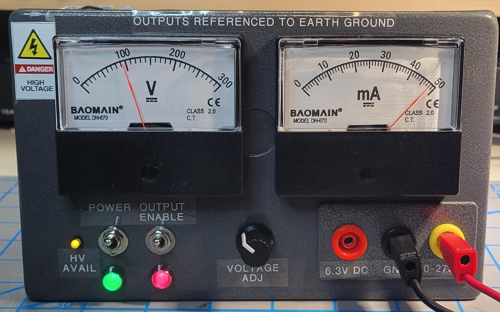
High-voltage power supply supplying 100V to a 2K load
I decided I needed a [moderately] high voltage power supply for my home lab. I have a number of lab supplies but the highest voltage I had available was about 55V. I wanted a supply I could use for project using Nixie tubes and vacuum fluorescent displays. Vacuum fluorescents can require up to 70V while Nixie tubes require 170 to 200 volts. So I decided to build my own. (Amazon sells one for a few hundred dollars but where’s the fun in that?)
Initial Research
I started by doing an Internet search and found a number of designs for high-voltage power supplies, most of which were intended for use with vacuum tubes which typically require 6.3V for the filament, about 300V on the anode, and a negative voltage for the grid. I found a possible design by Chappy Happy on YouTube based on an adjustable 12V to 45 to 390V boost converter module. (This module can be purchased with either a single output or with complementary outputs. The only difference is the dual output version includes an additional output rectifier diode and filter capacitor for the negative output and replaces the two-output terminal block with a three-output block.)
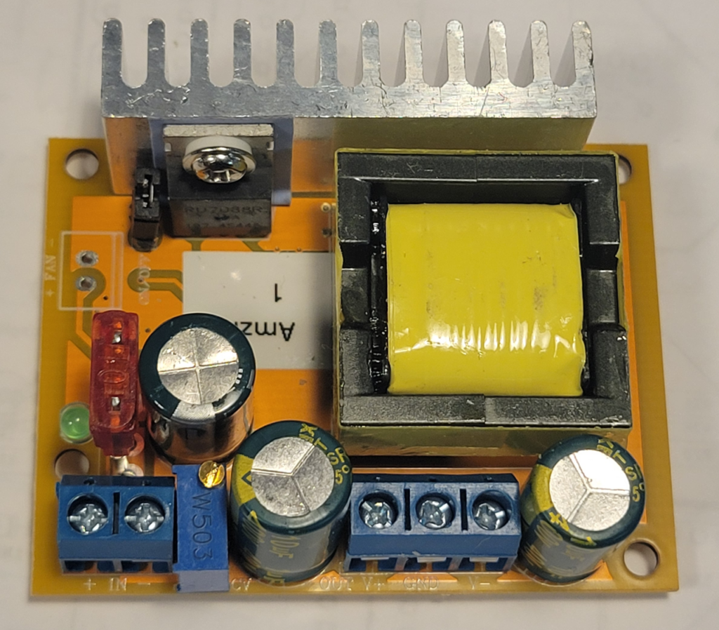
Dual Output DC-DC High Voltage Boost Converter
I purchased a pair of these from Amazon for $10 and tested them with 12V input. My plan was to replace the on-board, 10-turn trimpot with an external panel mounted voltage adjustment potentiometer. Unfortunately, at several voltage settings the output oscillated, in some cases by more than 20 volts. While it is possible this was because the output was unloaded, it makes the converter unusable as a lab power supply where the output load can vary from open to short circuit. (The latter not necessarily intentionally.) I then considered using one of these set to a fixed 300V followed by a high-voltage regulator to adjust the output.
There is a circuit in The Art of Electronics (Figure 9.17 reproduced below) for a variable high-voltage regulator built from an LR8 adjustable three-terminal linear regulator. The LR8 is designed around the same concept as the LM317 (see §11N.2 in LAoE) except that, rather than being limited to a maximum of 40V from input to output and supporting an output current of up to 1.5A, it allows an input-to-output differential of up to 450V but is limited to an output current of ~20 mA. The circuit in AoE adds a MOSFET follower to the LR8 to support higher output current. [2]
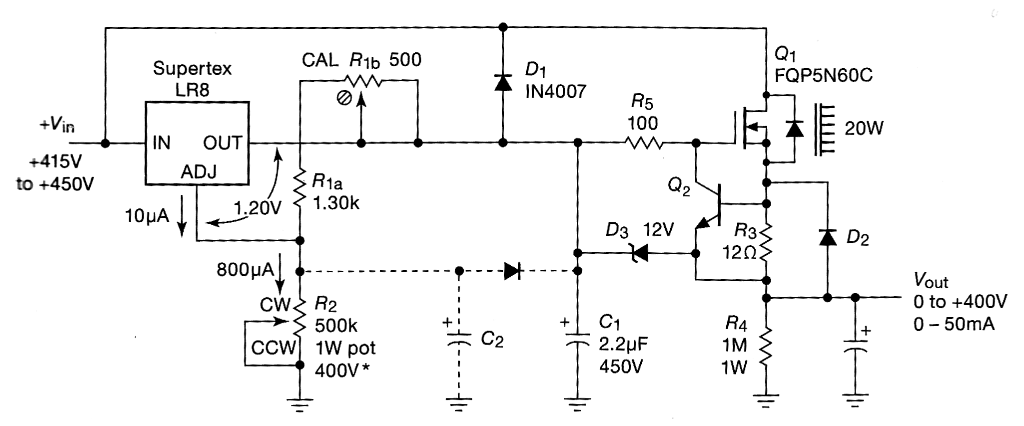
AoE Figure 9.17 High-voltage adjustable supply, 0 to 400 V, implemented with a low-current LR8 plus outboard MOSFET follower. Used with permission.
I contacted Winfred Hill (co-author of The Art of Electronics along with Paul Horowitz) with some questions about this circuit and he discouraged me from using the 12V boost converter, responding
“[This DC-DC converter] is badly flawed, non-functional compensation, etc. The flyback step-up ratio is 30-CT, way too high. I have given up on using it. What’s really needed is 120Vac input anyway.” [3]
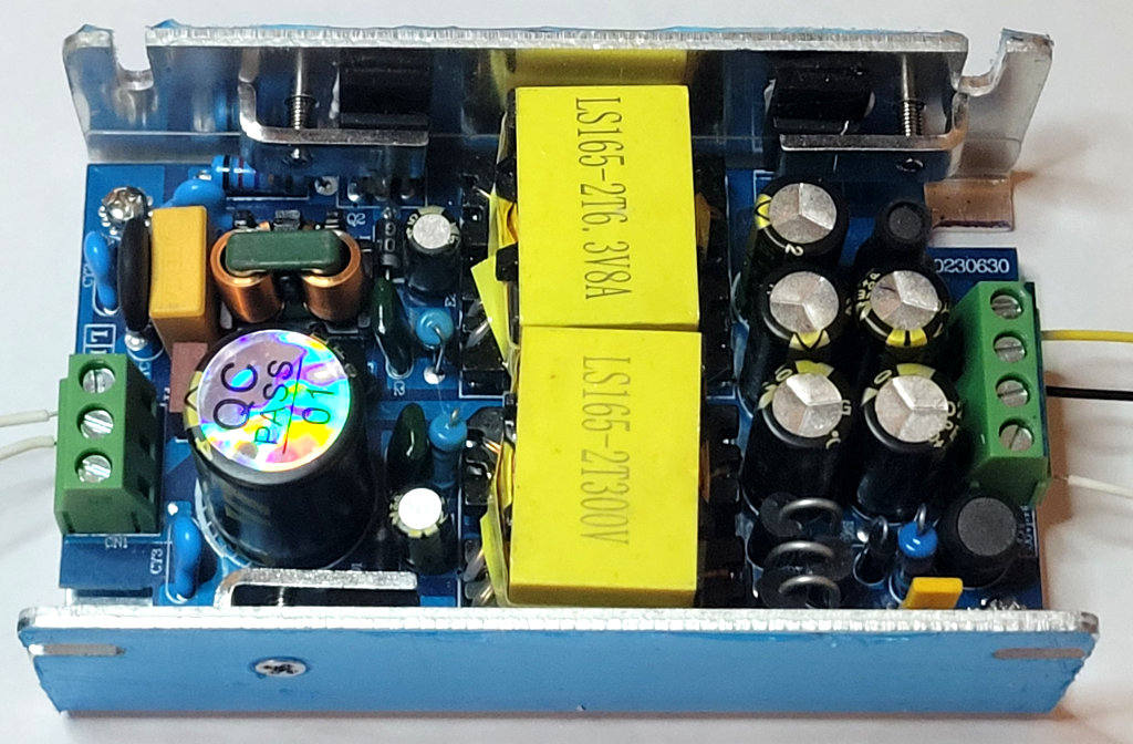
Vacuum Tube Switching Power Supply AC 100-265V to 6.3V 5A, 300V 300mA
I bought one of these ($30 at Amazon) and it worked just fine, although the output is closer to 280V than 300V. The only annoyance is that while the 6.3VDC output comes on immediately, there is an approximately 20 to 30 second delay after power is applied before the high-voltage output turns on. (This is deliberate to allow the filaments to warm up when used with vacuum tubes.)
The Voltage Regulator
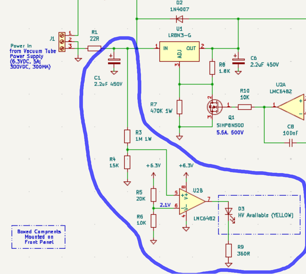
I rarely build a circuit in its entirety when I am working on a new project, even when based on a circuit I know will work like the one in AoE. Instead, I try to build the minimum necessary to see whether it will work for my application and to see if I have to make any modifications. I first built the basic LR8 voltage regulator circuit without the MOSFET follower (i.e., the circuit circled in blue in the schematic below). I needed to modify the circuit to output 0 – 300V since that is the maximum I could get out of the Vacuum Tube Power Supply (VTPS), so I changed resistor R1a to 1K to give an adjust current of 1.2 mA (which exceeds the minimum output current specification of 0.5 mA). That allowed me to use a standard value potentiometer (250k) for R2 to get a 300V range. (Had I kept R1a at 1.3K, I would have needed a 325K pot for R2 as noted — not a standard value.)
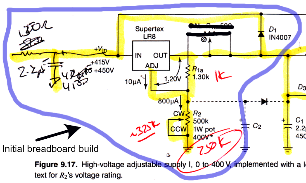
The first circuit I built was just a simple voltage regulator using the Supertex LR8
I did not immediately test this circuit with the 285V output of the VTPS. While the VTPS output is current limited, it still is capable of putting out almost 100W, enough to create a lot of excitement if I built the circuit wrong or a component fails. Instead, I first connected the circuit input to a lab power supply capable of providing ~55V but with adjustable current limiting set to about 10 mA (a bit over 500 mW).
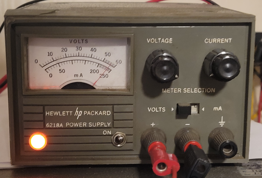
The 55V lab power supply I used initially to test the LR8.
Once I was satisfied the circuit worked, I replaced the HP supply with the VTPS.
This worked but there were a couple of issues that bothered me. First, AoE recommends at least a 1W pot for R2. I used a linear 250K, 1W potentiometer for the build but I was unsure if I would prefer a logarithmic or reverse logarithmic pot to get a good adjustment feel over the full output range. I had both but they were only rated for 1/4W. Second, I really did not like bringing the full 300V to the front panel and near my fingers. The potentiometer was rated for the full voltage but I still prefer not to have high voltage on an adjustment control. Finally, as AoE explains, the output of the LR8 is set by the potentiometer but the actual output voltage is reduced by the MOSFET follower gate-to-source voltage (AoE adds a trimpot to trim this out but it is a bit of a kludge to keep the circuit simple). Since I had an additional 6.3V available from the VTPS, I decided to use that to correct all these issues.
In my next iteration, the output voltage is sensed by a voltage divider and compared to a reference set by the wiper of a potentiometer forming an adjustable low-voltage voltage divider. One-half of an LMC6482 rail-to-rail, single-supply op amp drives a high-voltage MOSFET to set the LR8 ADJ voltage so that the divided output voltage matches the potentiometer output. The 470K resistor from ADJ to ground sets the maximum output voltage should the MOSFET fail. [4] Note that the negative feedback path is to the positive terminal of the op amp because the MOSFET is inverting, higher gate voltage reduces the ADJ voltage. The 680 nF capacitor around the op amp stabilizes the feedback loop (the 100 nF capacitor from the gate to ground was not needed and is not installed). The 100K and 10K resistors at the input and output of the op amp isolate the compensation capacitors from low impedance sources to allow the compensation to work.
The adjustable regulator with feedback from the output added
Again, I first tested the circuit with the HP lab supply before replacing it with the VTPS. The voltage adjusting MOSFET dissipates less than a watt at the highest output voltage, so I initially used a STQ2LN60K3-AP 600V, 2.5W MOSFET in a TO-92 package. However, it got uncomfortably warm in free air so I replaced it with a SiHP8N50D, a 550V MOSFET in a TO-220 package.
Once I was sure the feedback circuit worked, I added the MOSFET follower from the AoE design and moved the feedback divider to the new output of the circuit. Again, I first tested the circuit with the lab power supply before connecting the VTPS. The result is a circuit that compensates for the MOSFET Vgs, only applies 6.3V to the front panel pot, and allowed me to try both logarithmic and reverse log potentiometers to see which gave me the voltage adjustment I liked best (which turned out to be the linear pot). Since I had a second op amp in the LMC6482 package, I used it as a comparator to indicate when the high-voltage supply was available. [5]
High-voltage available indicator circuit
However, the long power-on delay before high-voltage is available from the VTPS presented an additional problem. Once I have a circuit-under-test working, I want to be able to turn the power to it on and off as I make changes and/or adjustments to it. Normally, I can just switch off the power supply but with the VTPS, the 30 second delay would make modifying and troubleshooting frustrating. I needed a way to switch the output of my high-voltage power supply on and off without having to fully power it down. This is harder than it sounds. Mechanical switches are usually rated to switch up to 240V AC but often are limited to only 30V DC. [6] Additionally, as with the potentiometer, I prefer to keep high voltage away from user controls.
I first considered using a solid state relay (SSR) to switch the output on and off. A solid state relay is a packaged device with a set of light sensitive MOSFETs separated from one or more LEDs by an insulating but light permeable material. Lighting up the LED with a low voltage switches the MOSFETs to their conducting state, turning on the switch. I found a SSR capable of switching 1500V at up to 50 mA that seemed like it would work to switch my power supply output. Unfortunately, the on-resistance of this device was spec’ed at a maximum of 200Ω (100Ω typical). At the maximum output current of my power supply, the voltage drop from the relay alone could be as high as 10 volts and would vary with current drawn. I decided to keep looking for a better solution.
Luckily, I stumbled on a small mechanical relay rated to switch up to 300V DC at up to 50 mA with a contact resistance of only 150 mΩ. However, the relay is limited to switching a maximum of 10W, meaning you can use the relay to switch the maximum current of 50 mA up to an output voltage of 200V. Above 200V, the allowable current derates linearly until it reaches 33 mA at 300V output. Nevertheless, it seemed to me like the best solution to switching the output of my high-voltage power supply — I will just have to avoid operation outside the 10W envelope.
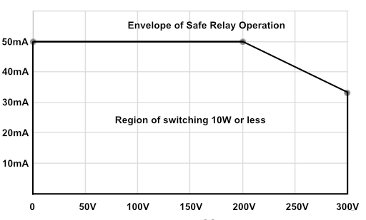
Operating VI envelope of the high-voltage relay
One end of the relay coil is connected to 6.3V and a front panel switch grounds the other side of the coil through a 130Ω resistor to turn the output on. The resistor drops the coil voltage to its rated 5V. [7] I also added a red LED on the front panel to indicate when the output voltage was enabled.
The Front Panel Meters
I wanted both a voltage meter and a current meter to monitor the output of the power supply. I found a nice analog 300V meter to monitor the voltage but I could not find a corresponding 50 mA meter for the current. I did find a matching 1 mA meter that I modified to measure 0 to 50 mA. I first used a resistance substitution box and lab power supply to set the 1 mA meter to full scale and then measured the voltage across its terminals at 160 mV. Since I wanted the meter to read full scale when a total of 50 mA total was flowing, I needed a shunt (i.e., a resister in parallel with the meter) that would pass 49 mA with 160 mV across it. Dividing 160 mV by 49 mA gives 3.27Ω so I added a 3.3Ω shunt resistor. I also replaced the meter scale with one I made up reading 0 to 50 mA.
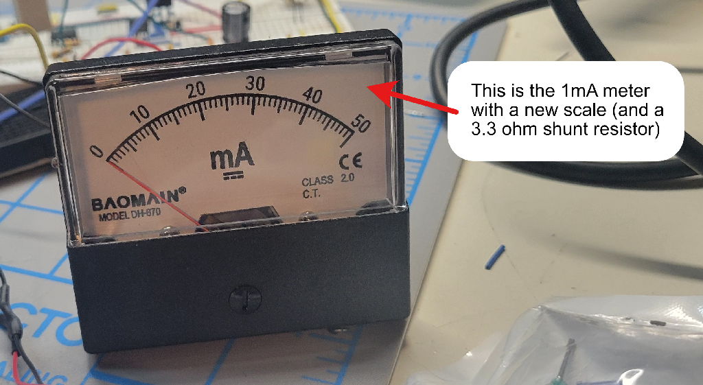
1mA meter rescaled for 3.3 ohm shunt resistor
The Final Design
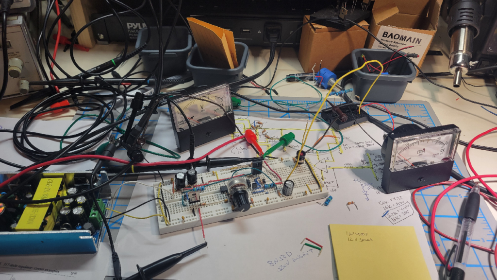
I built and tested the design in stages on a single breadboard strip. Initially I used several 1W resistors in series as a load. You can see these on the small black breadboard in the upper-right in the figure below. (I later bought a kit of 10W resistors so I could test the final build at higher voltages and currents.)
Test of high-voltage regulator breadboard before addition of output switch and HV available circuit.
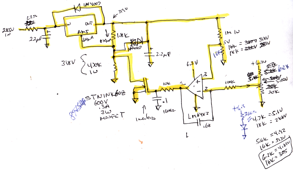
Here is the final schematic of high-voltage power supply. (VTPS not shown.) [8]
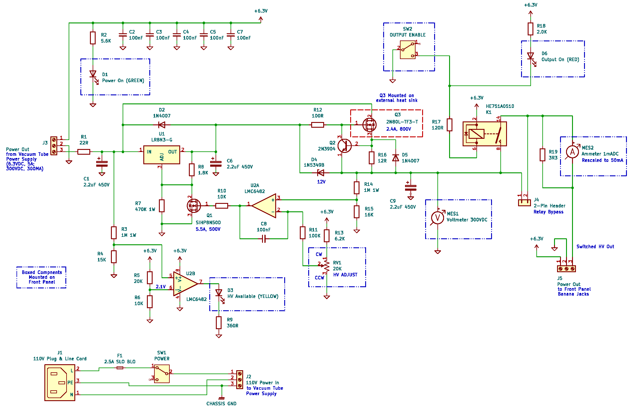
Schematic of the high-voltage power supply breadboard before initial testing
I considered designing a printed circuit board for the power supply but decided it was too much work for a one-off. I ended up building the final circuit on an Adafruit Perma-Proto breadboard.
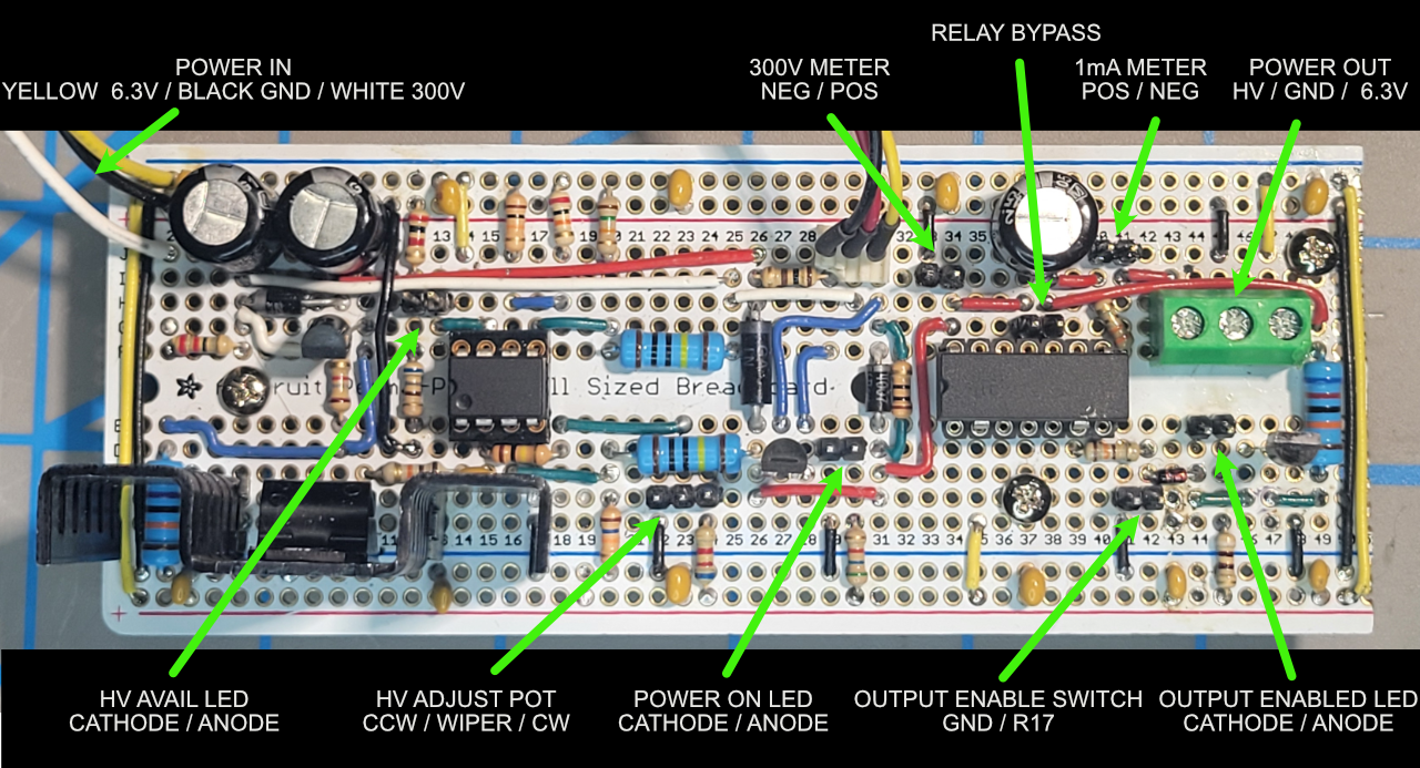
External connections labeled with second line showing individual connections from left to right
Choosing a Heat Sink
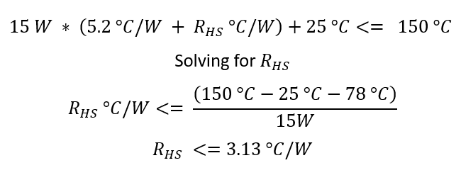
Since this is a linear power supply, the power dissipated is always the VTPS output voltage (~285V) times the load current. This power is split between the load and the pass transistor, Q3, depending on the output voltage. The higher the output voltage the lower the power dissipated in Q3. Worst case pass transistor dissipation of about 15W occurs into a short circuit where the voltage across Q3 is 285V and the current is approximately 50 mA (set by the current limiter formed by R16 and Q2). The 2N80L-TF3-T is an 800V, 2A MOSFET in a TO-220F package. This package has a junction-to-ambient thermal resistance of 62.5 °C/W and a maximum allowed junction temperature of 150 °C. At 15W times 62.5 °C/W, the junction temperature would greatly exceed the maximum allowed in free air, so I had to mount Q3 on a heat sink. The junction-to-case thermal resistance is 5.2 °C/W, and if we assume an ambient temperature of 25 °C, the heat sink must have a thermal resistance less than 3.13 °C/W.
The heat sink must also fit the back of the case (described below). I chose an Adam Tech HSK-055-05 TO-220 heat sink with a thermal resistance of 3.00 °C/W. This does not leave much temperature margin but I did not have room for a larger sink. In general, I think it is unlikely I would be using this power supply if my [much better] 55V HP supply shown above was adequate, so the only time it is likely to have full VTPS voltage and full output current across the pass transistor is if there is a short circuit and I assume I would shut down the supply quickly if that happens.
I tested the heat sink selection with a power supply output of 100V (185V across the pass transistor) and a 2K, 10W load resistor (50 mA) and measured 51 °C on the heat sink implying a junction temperature of about 100 °C. With a 1K load resistor and 50V output (still 50 mA), I saw heat sink temperatures of about 68 °C implying a junction temperature of about 130 °C. Since I do not expect to use this supply at voltages less than 50V, this heat sink seems acceptable. [9]

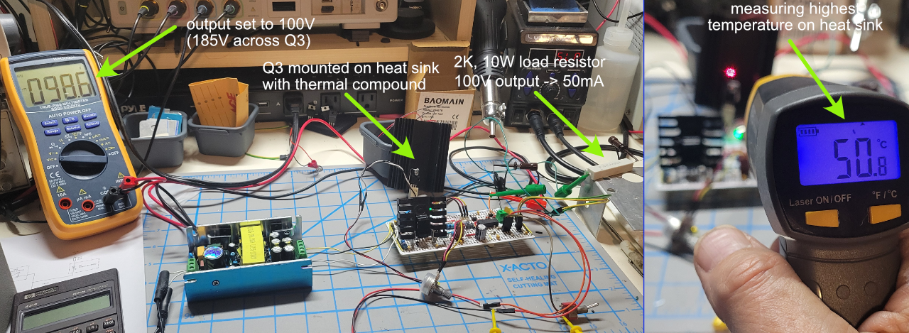
Testing Q3 heat sink temperature rise
Packaging
A project is not over until it is in a box. The VTPS, circuit board, heat sink, meters and switches would not fit in even the largest size of my favorite project box but I liked the Heathkit QF-1 box Chappy Happy on YouTube used for his version (see video at 2:52). I found an identical Heathkit Q Multiplier on eBay and gutted it to use to package my power supply. The Heathkit case uses a clever design. The front panel is attached to an internal U-shaped chassis by the front panel controls and all the other electronics are mounted to this chassis. The rest of the enclosure is a rectangular box with one face (the front) missing that attaches from the rear with two screws into the chassis. There are no components attached to the rear box and it has holes to allow wires from the internal chassis to pass out the back.
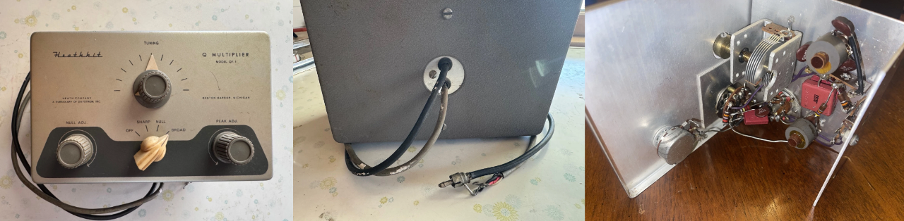
Front, back, and internal chassis of the Heathkit Q Multiplier I bought on eBay
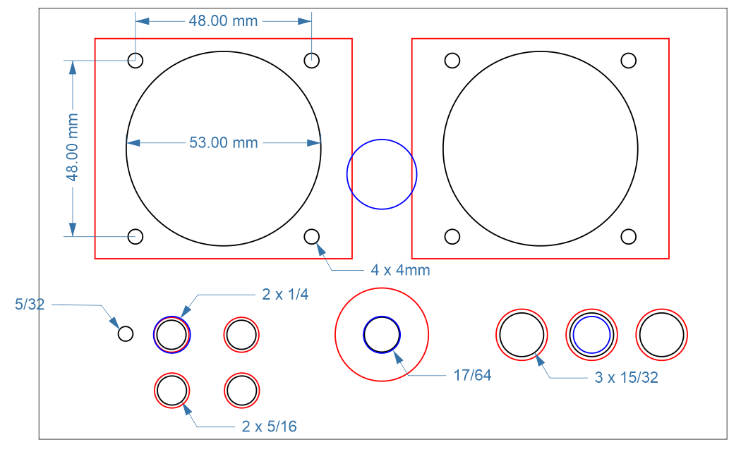
I started my mechanical design by using CorelDRAW to layout a rectangle the size of the existing Q Multiplier front panel. I then added all the power supply front panel controls, trying to reuse existing holes as much as possible. In the drawing below, the blue circles are the existing holes, the black circles are the new holes for the power supply controls, and the red represents the outlines of the power supply control and display items that go in each hole. My final design used all the existing holes except for the one in the center.
CorelDRAW front panel design for high-voltage power supply
I imported this mechanical image into my drawing program (Affinity Photo) and added images of the controls to make sure I was happy with the layout.
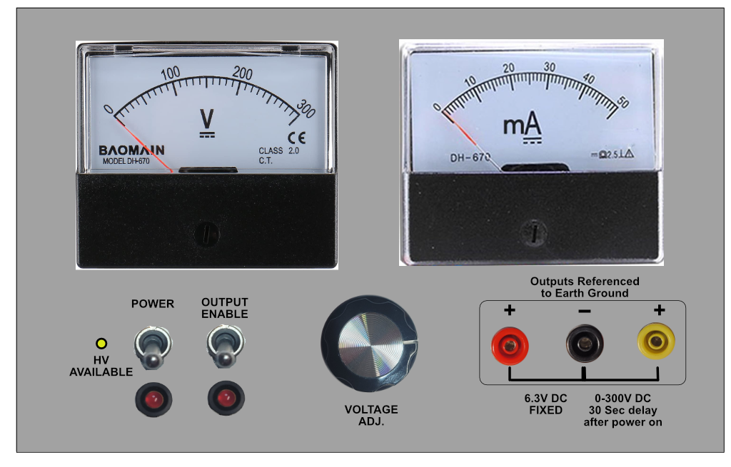
Mockup of front panel of finished high-voltage supply
Once I was satisfied with the aesthetics and ergonomics, and had checked to make sure there was room for all the parts, I made up a new internal chassis to replace the original one. I then temporarily attached the original Q Multiplier front panel with screws through the meter mounting screw holes and cut holes in the front panel to match the ones on the internal chassis.
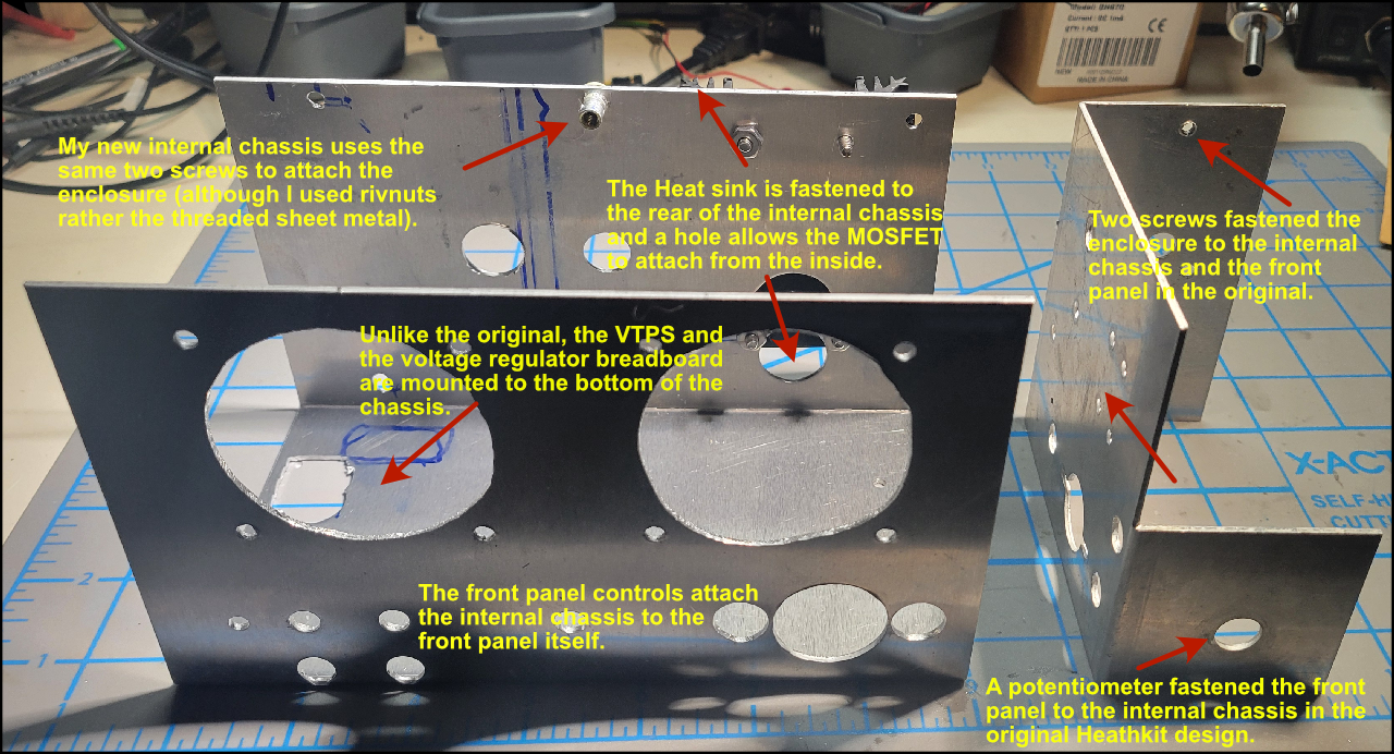
Comparison of the new Heathkit Q Multiplier internal chassis (left) with the original (right).
Original Q Multiplier front panel attached to new internal chassis with holes cut to match
Finally, I powder coated the front panel with my favorite hammertone gray finish.
The final fabrication step required adding two additional openings to the back of the rear enclosure for the fuse holder and the MOSFET heat sink.
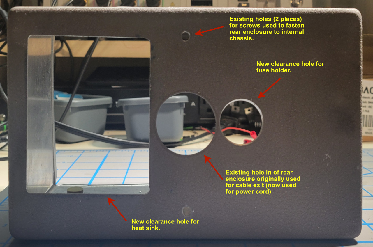
Rear enclosure with added openings for heat sink and fuse holder.
Assembly
Once the packaging was complete, all that was left was to assemble the parts and test the final product. I began by installing the power components including the line cord, fuse holder, VTPS, power switch, and voltage regulator breadboard with Q3 fastened to the external heat sink.
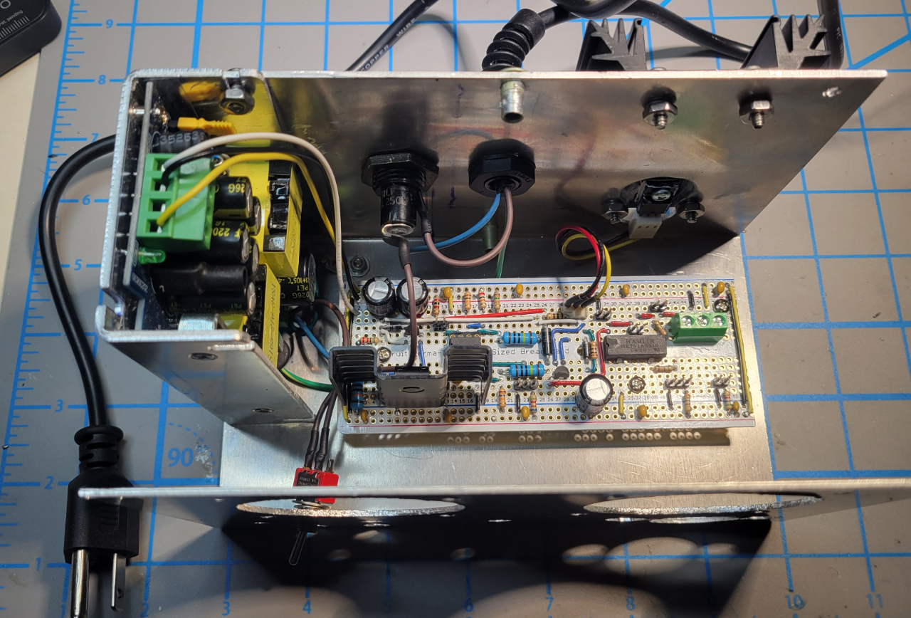
Internal chassis with voltage regulator, VTPS, and power wiring installed and Q3 mounted to heat sink.
The remaining front panel control were added to hold the front panel to the internal chassis followed by the panel meters. [10]
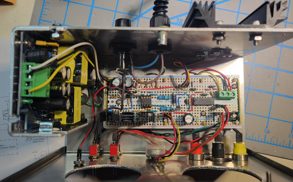
User controls installed through both chassis and front panel
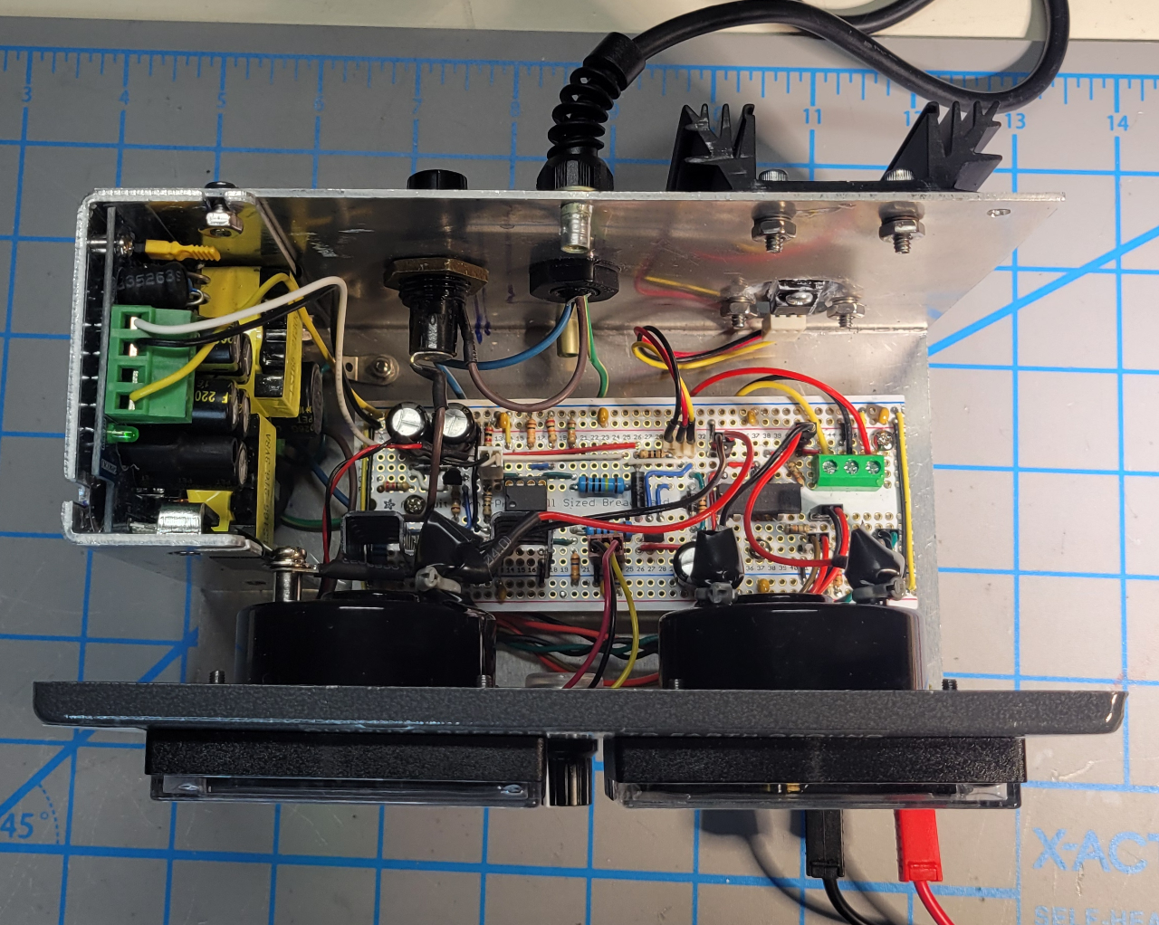
The electrical build is finished with the addition of the panel meters
I then added the high-voltage warning and front panel labels and screwed on the rear enclosure before I tested the power supply.
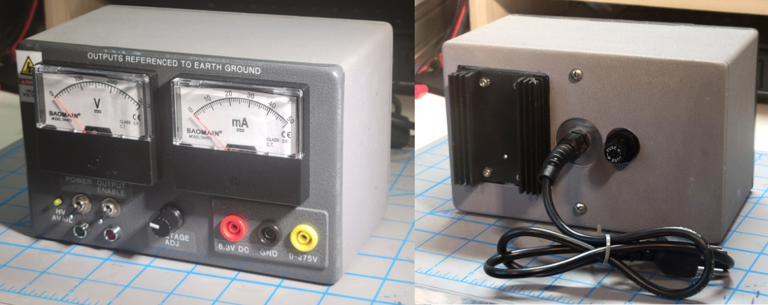
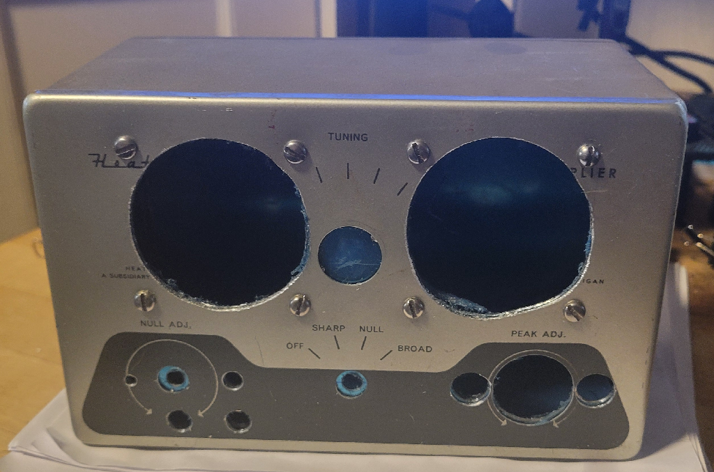
Front and back views of competed high-voltage power supply
Testing (updated 2026-02-10)
In initial testing, the supply seemed to work well and I was pretty happy with the result. Here it is supplying 231V to a 4.7K resistor (~50 mA). The switching noise is about 2V peak-to-peak (it drops to half that with no load).
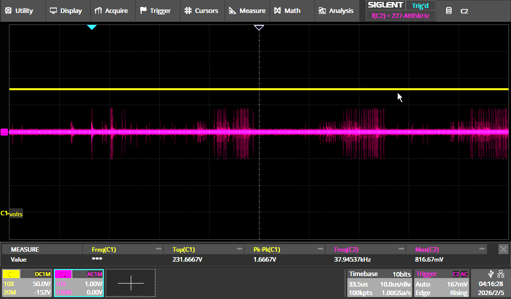
Completed power supply providing 231V into a 4.7K resistor (50 mA). Second trace is AC coupled to show switching noise.
I thought I was done but Paul Horowitz suggested I needed to measure the transient response to a step load and also make sure that the supply was stable driving a capacitive load of at least 10uF or 50uF.
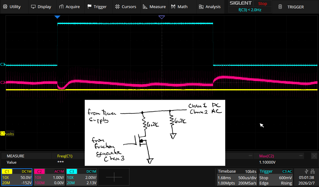
Step response of power supply output to a 20mA change in current (original design with reed relay)
I set up a simple test jig to switch the load between ~20mA to ~40mA to measure the step response with a ~124v output.
Unfortunately, after completing these tests I noticed that output was still live, even though the OUTPUT ENABLE switch was in the off position. Sometime during my testing the high-voltage output relay contacts had become stuck in the closed position. Paul suggested the failure occurred because the output capacitor, C9, was after the current limiter circuit but before the output relay. This allowed excessive current to flow through the relay when the contacts closed and the output was connected to a capacitive load. Indeed, I later found this warning on the data sheet for another manufacturer’s high-voltage reed relays:
Pickering Relay datasheet warning concerning capacitive loads
The solution, was to move the capacitor to after the output relay switch so current flowing from it to charge capacitive loads would not flow through the relay. This change requires adding a discharge resistor in parallel with C9, to make sure the output voltage decays to zero when the supply is turned off, even if there is no resistive load attached.
However, the relay failure exposed an even more serious hazard in my design. The accompanying red warning LED extinguished when I turned off the output switch, even though the output was still live. The problem was that in the original design, the LED was controlled only by the OUTPUT ENABLE switch. If the switch was off, so was the LED even if the relay failed closed. To warn users of the presence of high-voltage, the LED must indicate the actual state of the output voltage. I added the following output voltage sense circuit to the LED control.
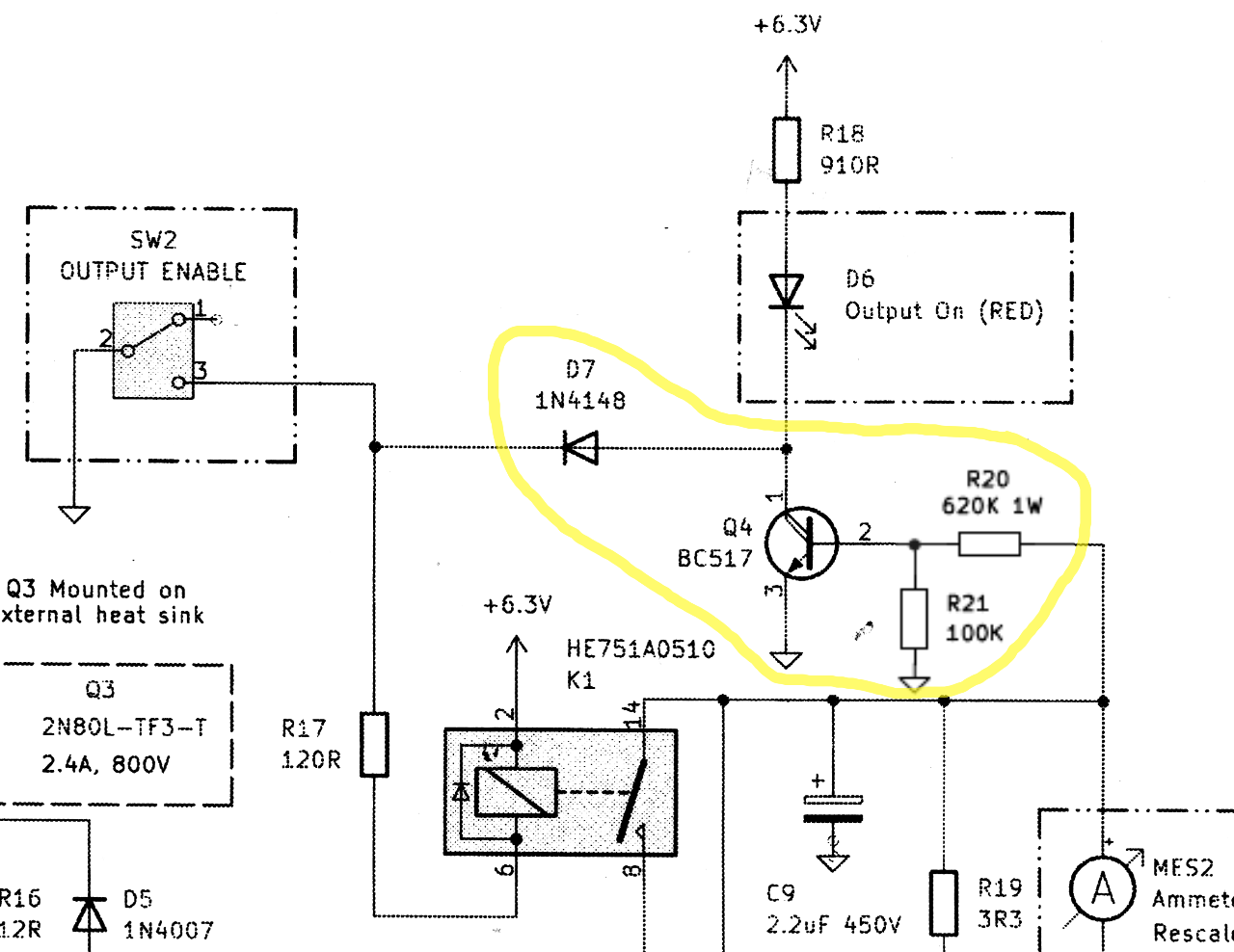
Output voltage sensing circuit turns LED on if output voltage > ~10V
This circuit uses a high-beta (>30,000) Darlington switch sensing the power supply output through a 620K/100K resistive divider. As long as the output voltage is more than ~10V, Q4 will be on and the LED will be lit even if the OUTPUT ENABLE switch is off. R20 and R21 provide a discharge path for C9 as well, eliminating the need for a separate discharge resistor. D7 is included so that the LED will be lit anytime the OUTPUT ENABLE switch is on, even if the output voltage is zero. (Without the diode, the relay would be energized whenever Q4 turns on and there would be no way to turn it off other than turning off the power to the supply.)
I added this circuit to my breadboard and tested it only to be surprised that the new relay I installed failed with the contact closed as well. Paul suggested it was because it possibly was marginally spec’ed. I decided to replace the reed relay with the VORA1150 high-voltage solid state relay (SSR) and live with its higher on resistance.
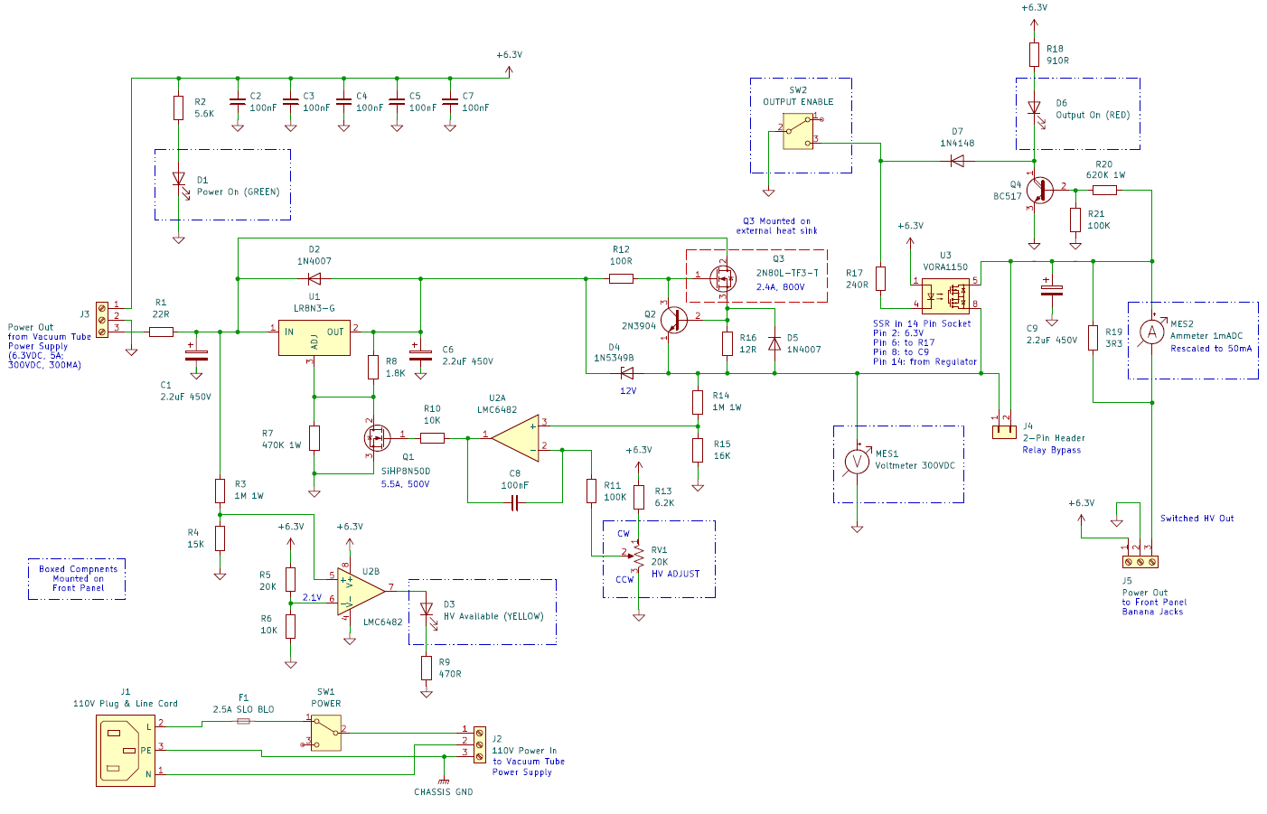
Final high-voltage power supply schematic with solid-state relay and output voltage sense circuit
I repeated the step and capacitance load testing performed on the original circuit. The supply was still stable with capacitance loads up to 120uF. DC testing showed the SSR had an on-resistance of 116Ω. You can see the effect this has in the load step test below.
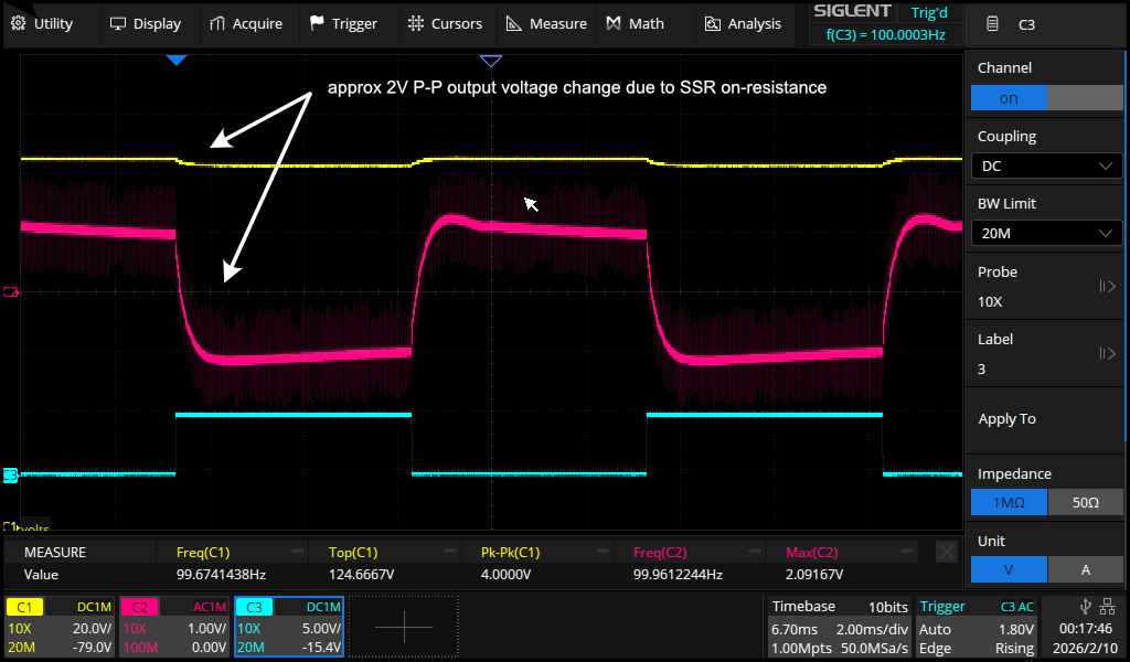
Response of high-voltage power supply using the SSR to a 20mA load change
The settling time appears to be the same, but there is now a change in the DC output voltage due to the on-resistance of the solid-state relay. I don’t expect this to be a problem with Nixie tubes or vacuum florescent displays since the change is likely too small to perceptibly affect the display brightness.
Acknowledgments
Thanks to Paul Horowitz and Winfield Hill for their comments and suggestions on the electrical design. Also thanks to Steve Sansone in the Harvard Instructional Machine Shop for his help on the packaging modifications.
David Abrams
mru 2026-02-10
Footnotes
[1] See Work Safely With High Voltage and Working with High Voltages.
[2] For an alternate solution to this problem, see National Instruments Linear Brief 47 which uses an LM317 to create an adjustable high voltage supply. This design limits the maximum voltage across the LM317 to about 5V with a Zener diode while dropping the remaining voltage across a pair of high voltage BJTs.
[3] Win also noted:
“If you have the bipolar version, remove the negative-side diode. With no neg load, its voltage can soar past 500V as you apply a positive load. The unipolar version certainly suffers from excessive voltages on the transformer winding, but I suppose it survives.”
[4] The 470K resistor dissipates less than 1/4 watt worst case but must be specified as a one watt resistor because it sees almost the full 285V at the maximum output voltage setting. One-quarter watt resistors are usually rated for less than 250 volts.
[5] The final design includes a voltmeter that would come alive when the high voltage becomes available if the power supply is not set to zero. However, I normally like to start testing a new circuit with the supply set to zero volts and increase the voltage slowly so I can stop immediately if something goes wrong (like the ammeter indicating excessive current draw). The yellow high voltage available LED lets me know when I can start testing in this case.
[6] The reason for this is because when the metal contacts start to move apart in a switch which is conducting electricity, an electrical arc forms between the contacts as they separate. This arc is self-extinguishing with AC circuits because the voltage always goes to zero within one-half cycle of the power line. With DC circuits, the voltage stays constant, causing the arc to persist and possibly damage the switch.
[7] While the relay coil itself is not polarized, this version of the relay includes an internal clamping diode so the 6.3V supply must be connected to the coil pin connected to the diode cathode.
[8] You may be wondering why I used two different high-voltage power MOSFETs for Q1 and Q3? Q1, the SiHP8N50D adjusting the LR8 voltage regulator, is supplied in a TO-220 package while the 2N80L MOSFET output follower is in a TO-220F package. The difference is the back and tab of the former is bare metal connected to the drain of the MOSFET (in a BJT it would be connected to the collector) while the tab of the TO-220F is insulated from the drain.
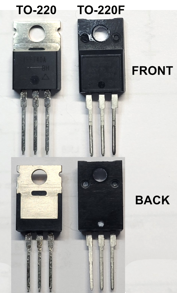
Since Q3 is fastened to the external heat sink, the heat sink would be at the full VTPS voltage of 285V unless an insulating mica washer and nylon screw is used to attach it to the heat sink if it was in a TO-220 package (I have mica insulators and #6 nylon screws but did not have a 3mm nylon screw). By using the MOSFET in the TO-220F package, I did not have to worry about the heat sink (which is accessible with the case closed up) of ever being connected to dangerous voltage. Since Q1 is inside the enclosure, it does not matter that at higher voltage settings, the tab could shock someone if they touched it. The disadvantage of the TO-220F case is it has a much higher Junction-to-Case thermal resistance than the TO-220, resulting in a higher MOSFET junction temperature with a given power dissipation. The 2N80L has a Junction-to-Case thermal resistance of 5.2 °C/W, while the Junction-t0-Case thermal resistance of the TO-220 case of the SiHP8N50D is only 0.8 °C/W. Using the TO-220 device inside the case keeps the junction temperature of Q1 lower than if I used the same part as Q3.
[9] Note that these readings are at the maximum current available. At lower output current the junction temperature would be lower. In addition, in the final packaging the heat sink is fastened to the aluminum chassis, providing additional cooling to Q3.
[10] Sigh. You may be wondering why the color of the front panel output jacks do not match the color of the internal wiring (the 6.3V internal wiring is yellow while the external jack is red and visa versa for the high voltage output). This is just poor planning and me not thinking the entire project through from the beginning. I normally use yellow for analog voltage and red for digital in my projects and it wasn’t until I started final assembly that I realized I wanted the high-voltage output jack to be yellow to match the high-voltage warning label. C’est la vie.