
Designing a breakout board for the LTC3261 charge pump
I have been working on an upgrade to my high-voltage lab power supply to add an adjustable current limit feature. The initial design ran all the op-amps on a single-supply using the low-voltage 6.3V supply available from the vacuum tube power supply; however, the upgrade requires an AD8479 instrumentation amplifier (see LAoE Section 7N.6) running with symmetrical dual supplies of +/-6.3V. Since the current required by the AD8479 is less than one mA, it does not make sense to add another power supply, rather the “flying capacitor” analog switch configuration of Figure 12L.12 (often called a “charge pump”) can easily provide adequate current for this application. I decided to use the Analog Devices LTC1044 Switched Capacitor Voltage Converter (about $6.30) which can invert voltages from positive 1.5V to 9V and supply up to 20mA. Luckily, this part comes in an 8-pin DIP so it is easy to use in a breadboard.
While I was researching charge pumps, I came across an interesting part, the Analog Devices LTC3261 High Voltage, Low Quiescent Current Inverting Charge Pump. While somewhat more expensive (about $10.50) than the LTC1044, this part can invert voltages from 4.5V up to 32V and supply up to 100mA making it usable to power relatively complicated +/-15V circuits at higher currents from a single positive voltage. However, one problem with the LTC3261 is that it only comes in a very tiny 12-pin MSOP surface mount package. Another is that the only ground connection is an exposed pad on the underside of the device; none of the many unused pins connects to ground, meaning it always requires a custom printed circuit board (PCB). [1]
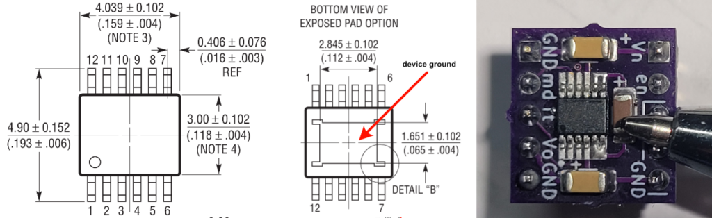
Dimensions of the LTC3261 12-pin MSOP surface mount package and its size compared to a ball-point pen. The upper dimensions are in mm while the lower dimensions in parentheses are in inches.
While I did not need the LTC3261 for this application, I decided to create a breakout board so I could breadboard with it in the future. [2] The recommended PCB foot print for the LTC3261 includes a 0.112 inch by 0.65 inch rectangle to solder to the ground pad on the underside of the device. In the normal automated surface mount device (SMD) assembly operation, a printed circuit board has solder paste applied through a stencil to the exposed solder pads, the SMD devices are then placed on the board and the assembly is heated in a temperature controlled oven until the solder paste melts and both connects the electronic devices to the circuit traces and mechanically fastens the components to the PCB.
When I manually assemble SMD devices, I apply solder paste to the pads and then use a hot air gun to melt it to form the joint. [3] This works on the exposed pins of the LTC3261 but does not reliable melt solder applied to the pad under the device. Jim MacArthur designed an alternate PCB footprint for the LTC3261 that includes a plated through hole (PTH) in the middle of the device pad to apply solder to the ground connection.
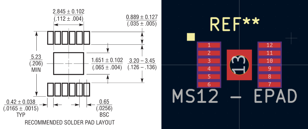
Comparison of the manufacturer’s recommended solder pad layout on the left and Jim MacArthur’s hand solderable layout on the right showing the addition of a PTH to provide solder access to the ground connection under the part.
A basic LTC3261 application requires an input and output decoupling capacitor along with the flying capacitor used to invert the input voltage (again, see LAoE Figure 12L.12). While I normally use the default configuration shown below left (EN to VIN; MODE and RT to ground), I added these three configuration connections to my breakout board’s pins rather than connect them internally to allow me to configure the LTC3261 differently if required in another application.
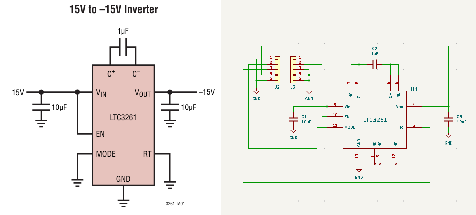
Standard LTC3261 inverter configuration and breakout board schematic, created in KiCad, showing control lines brought out to breadboard pins.
In my early days, we designed printed circuit boards by laying them out at 2x or 4x size on transparent mylar film with black tape (for single sided boards and pads on both single-sided and multi-sided boards) or red and blue tape for double sided boards. Indeed, some still refer to the process of laying out a PCB as “tape out.” Nowadays, PCBs are designed using computer programs to create a set of production files (“gerbers“) which are sent to a production house to manufacture the bare board (or in some cases to not only make the PCB but to populate it and optionally test it for you). There are a number of commercial PCB layout programs but I use KiCad, a free, open source a full-featured schematic capture, PCB layout, and 3D board viewing program. I first create the schematic of my breakout board in the KiCad schematic editor, assigned footprints (the actual PCB copper pattern) to the schematic symbol for each device, then use the PCB editor to position each component and modify the “rats nest” connections into copper traces of the correct width while avoiding crossovers which would short signals by using the front and back of the board and through component lead PTH and vias (small PTH used just to route signals from one side of the board to the other).
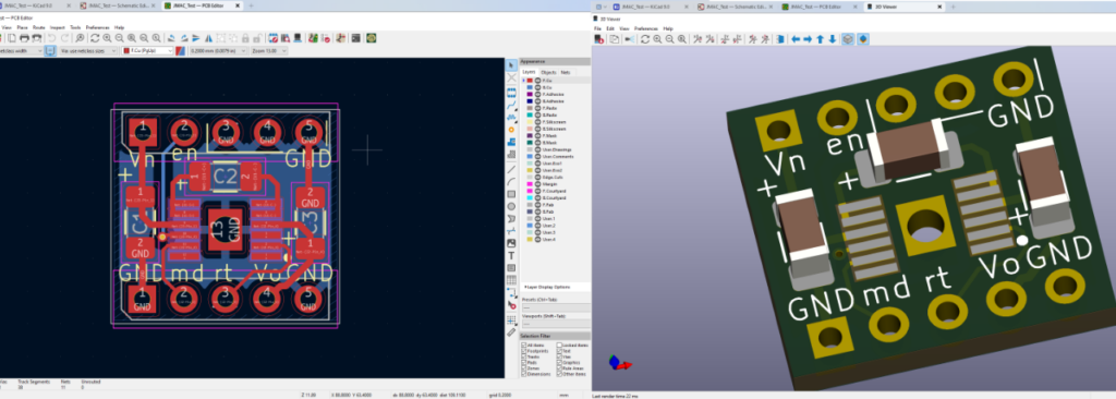
KiCad LTC3261 breakout board layout (left) and 3D rendering (right). In the layout, red is the front copper, blue is the back copper (matching the red/blue tapes of yore) with yellow the front silkscreen. The white lettering in the left image is for reference to the schematic and does not appear on the finished PCB.
KiCad includes tools to check your schematic and PCB layout for errors. (That is why the schematic is marked with Xs on unused pins — so they are not flagged as unconnected by KiCad.) Once I was happy with the layout, I generated the Gerber production files and looked for a company to manufacture the board.
In the first half of 2025, I used JCLPCB in China for printed circuit board manufacture. Their per-board price was much cheaper, often by an order of magnitude, than domestic manufactures, even with shipping charges. I typically received boards about a week after I uploaded the Gerber files to their web site. Unfortunately, on May 2, 2025, the Trump administration ended the de minimis tariff exemption for low-value imports from China. The actual added cost of the tariff is mostly inconsequential but the only way to pay it is to let a third party handle the payment to the US government. On a more expensive order the administrative charge for this service is still cheaper than the quote I got from a US company.
However, not only is the LTC3261 breakout board a very small (i.e., low cost) PCB, but I only need a few of them (I only bought three LTC3261s) making the administrative tariff charge uneconomical. So I decided to investigate domestic PCB producers. I first uploaded my gerbers to OSH Park, located in Lake Oswego, Oregon. They quoted a very reasonable $5.60 for 12 boards including shipping. I placed the order on June 8, 2026, and they shipped the boards to Boston on June 20th (12 days). Unfortunately, the shipment apparently was misaddressed and it was returned to Oregon and did not get back to me until June 30. In the meantime I received email from DigiKey promoting their DK Red PCB service. Worried I would never see the OSH Park boards, I placed an order with DK Red on June 26th for 10 boards at $4.57 including shipping. Also very reasonable. I received the DK Red board order on July 10, 2026 (14 days).
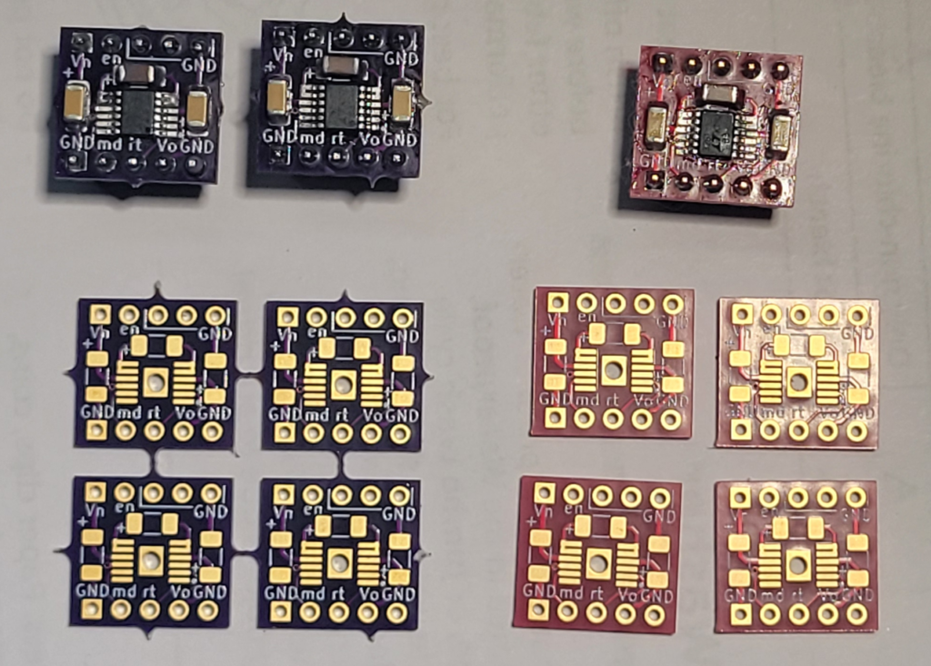
The OSH Park and DK Red breakout boards. OSH Park’s trademark is purple while DK Red’s is (not surprisingly) red.
The breakout board uses 1206 SMD capacitors. These are considered a “large footprint” SMD component at 3.2 mm × 1.6 mm (0.126″ × 0.063″) but are still hard to place without a set of precision tweezers. In addition, some SMD passive components such as these multilayer capacitors are not marked with a value. I bought a pair of DT71 Mini Digital Tweezers to confirm the value but you can get by with an inexpensive pair of multimeter lead tweezers. I have not tried them, but another choice priced between the two above is the FNIRSI LCR-ST Meter Tweezer available direct and on Amazon.
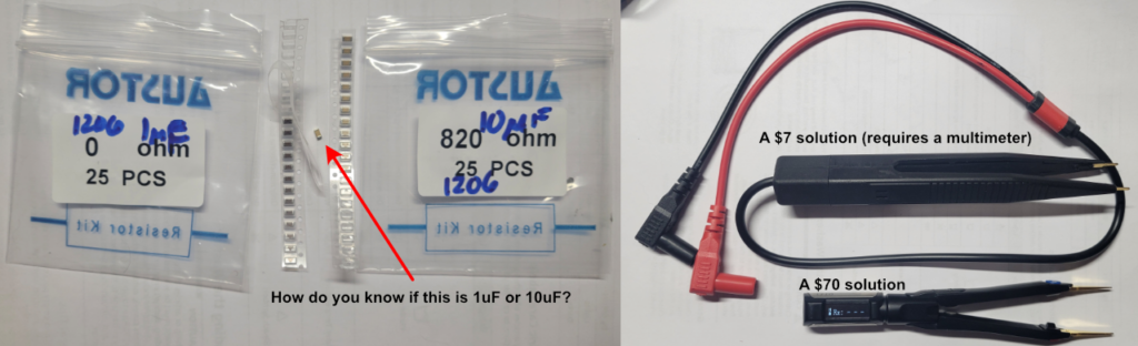
Not all SMD passive components are marked with a value. Here are the tools I use to make sure I am using the correct value. Note that the capacitance of these multilayer ceramic capacitors changes with applied voltage so don’t expect them to read exactly.
Both the OSH Park breakout board and the DK Red breakout board worked fine and the price was very reasonable for both. However, the price for a larger board (128mm by 109mm) I had previously had manufactured by JCLPCB was quoted by DK Red at $129.76 for four pieces shipped. I paid $60.32 for 10 boards shipped with tariffs for the same board from JCLPCB a year earlier. So it appears the domestic manufactures are a good choice for a small board where shipping and tariffs are likely to dominate but JCLPCB is still cheaper for larger jobs where the per board cost dominates.
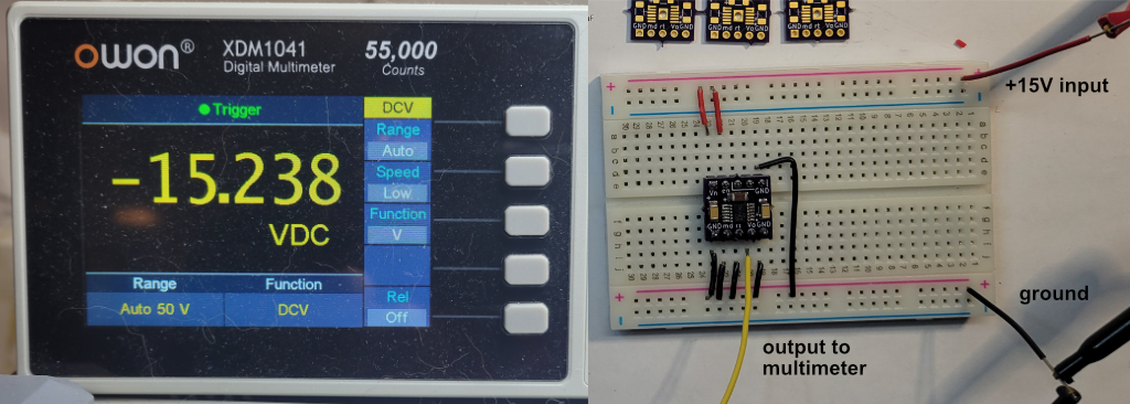
Demonstration of the LTC3261 breakout board with a +15V input.
The gerber files for the LTC3261 breakout board are available at https://laoe.link/LTC3261_Breakout_Gerbers.zip
Even if you don’t plan to order breakout boards, you can upload the .zip file to most manufacturers’ web sites to view the board’s layers including front and back copper, front and back solder mask, front silkscreen, board outline, and drill layer.
[1] Most likely, the reason for this is that at high output currents the device needs to dissipate more heat than can be removed through a pin. Soldering the body to a large PCB pad removes much more heat. The designers could have also assigned ground to a pin to allow the device to be used in low output current applications but apparently they did not trust their users. Unfortunately, this means you cannot use a standard MSOP protoboard to breadboard adapter with the LTC3261, even if your application requires only a few milliamps of the negative voltage.
[2] A breakout board is a small printed circuit board used to connect a surface mount device to DIP pins so you can breadboard with the device. See LAoE Figure 5L.3. Breakout boards can include additional support components to form a complete working system. LAoE uses an FPGA breakout board (Fig. 15L.1) in the digital lessons and an ARM microcontroller breakout board (Fig. 22N.10) in the microcomputer lessons.
[3] I purchased a combination soldering iron and hot air rework station along with a solder paste kit from Amazon. I keep the solder paste and flux in the freezer when I am not using it and let it come to room temperature when I do.