
Substitutes for the CA3096 Transistor Array
The CA3096 bipolar transistor (BJT) array used in Lab 5 of Learning the Art of Electronics is getting hard to find. It is no longer available from any of the major electronics distributors and surplus/obsolete distributors like Rochester Electronics LLC tend to require large minimum quantities. The CA3096 appears (as of 10/2025) to still be available in small quantities at reasonable prices from Amazon and on eBay but some European readers have had trouble ordering from these sources. Let’s take a look at alternatives. (Spoiler alert — you can use discrete 2N3904 and 2N3906 transistors to do almost all of the lab. If you want the benefit of matched input transistors, the onsemi NSS40301MDR2G for $1.24 is a low cost replacement for the CA3096 but requires an SOIC-8 to DIP adapter.)
Lab 5.1 The difference or differential amplifier
The CA3096 is an integrated circuit (i.e., a set of components created on a single piece of silicon) consisting of three NPN BJTs and two PNP BJTs. We use this part in Lab 5 first to build a differential amplifier, a dual transistor amplifier configuration that eliminates many of the disadvantages of the single transistor common-emitter amplifier in Lab 4L.5. In particular, it eliminates the complicated biasing scheme required for the common-emitter circuit in Figure 4L.6 and allows zero referenced inputs. Since an input coupling capacitor is no longer necessary, the differential amplifier can be used with DC signals. The differential configuration also reduces the effect of temperature on the circuit’s operation. This is because the two NPN transistors forming the differential input amplifier are electronically and thermally matched, that is they have very similar VBE vs IC characteristics (see Figure 5N.22) when at the same temperature. Since all the transistors in the array are on the same silicon and close together, they tend to always be at the same temperature. That means that temperature changes affect both transistors equally so the amplifier’s operating point does not change appreciably compared to the single transistor amplifier. Finally, the addition of the second input means you can use the differential amplifier to compare two signals and only amplify their differences, a property that turns out to be extremely useful to build circuits with feedback.
We then use the remaining transistors in the CA3096 to build a crude operational amplifier (“op-amp”) and show how using the second input on the differential amplifier to feed back a fraction of the output signal eliminates both the output offset of the common-emitter amplifier and the crossover distortion of the push-pull follower of Lab 4L.3.2.
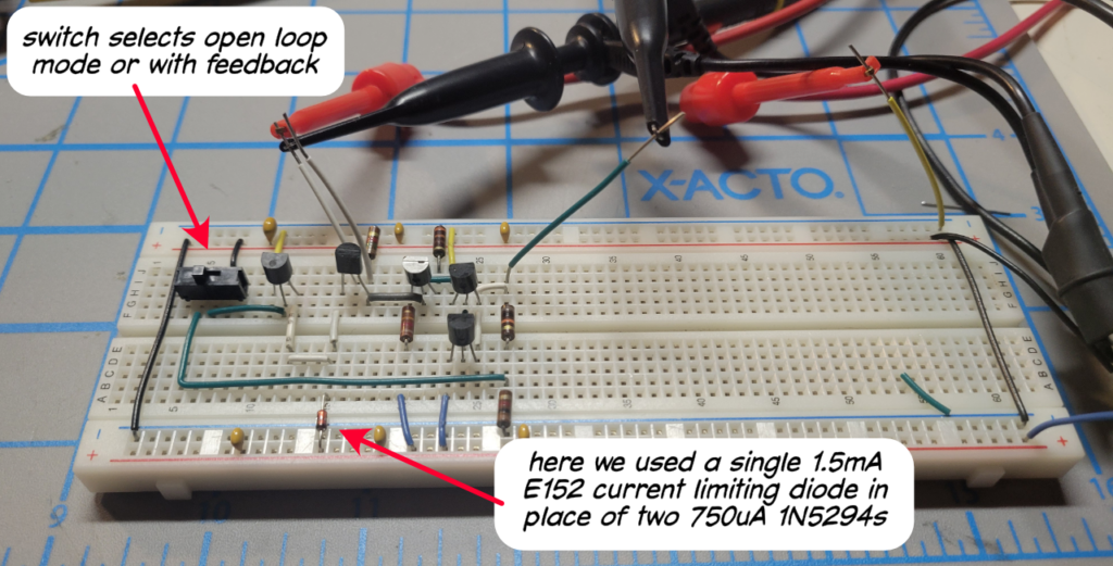
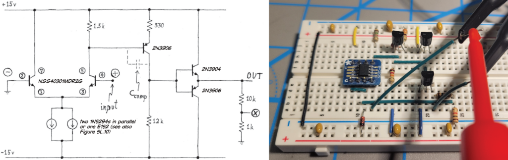
Another advantage of using the CA3096 is it mimics integrated circuit op-amps — all the circuitry is in a single integrated circuit (although real op-amps usually are in DIP packages with fewer pins since the connections are internal). Nevertheless, you can complete all the exercises in Lab 5.1 using discrete parts. Just substitute the 2N3904 for the CA3096’s NPN devices and use the 2N3906 for the PNP devices. Here is our completed op-amp (Figure 5L.15) built from discrete transistors. The slide switch selects either the open loop mode of Figure 5L.15 or the version with the feedback in Figure 5L.16. We used a 1.5mA E201 for the tail current which is why only a single part is needed.
Of course the discrete version of the differential amplifier cannot duplicate the electronic parameter matching of the transistors in the CA3096 array nor the close thermal coupling, but this does not really impact the lab. Indeed, it allows you to see a major benefit of feedback. When you test the final circuit of Figure 5L.15 open loop, try grabbing one of the input BJTs between your fingers to heat it up. You will see the DC level of the output drift as the VBE vs IC transconductance curve of that transistor shifts with the temperature change while the curve of the other BJT in the difference amplifier does not. See Figure 5N.14. The good news is that once you add the feedback of Figure 5L.16 this effect goes away (give it a try). As a colleague of mine used to say, “Feedback fixes everything” (see Chapter 6). In Chapter 7 you will discover that even real op-amps have small imperfections. These imperfections, such as input offset voltage and input bias offset, are worse using the discrete transistors in place of the BJT array but still remain small enough that you are unlikely to notice them in Lab 5.1.
If you would like to build the differential amplifier with thermally and electrical matched transistors and you are willing to solder surface mount devices onto a DIP carrier, you can find matched transistor pairs like the onsemi NSS40301MDR2G for $1.24 in a relatively easy to solder package using an SOIC-8 to DIP adapter. (There is also the National Semiconductor LM394CN, a matched NPN pair in an 8-pin DIP, apparently available from a Chinese distributor for $2.45 and on eBay and Amazon at higher prices but which we have not tried it yet.) Only the differential input NPN pair need to be matched. Here is the differential amplifier of Figure 5L.15 built with the onsemi dual matched BJT:
Lab 5.2 AM modulator
As with the differential amplifier, the AM modulator of Section 5L.2 can be constructed with discrete 2N3904 NPN bipolar transistors. The benefits of the transistor array are even less important here because the modulation input and modulated output are AC coupled. A slight variation in the transconductance curves between the discrete differential amplifier transistors results in a small variation in the quiescent output voltage which is removed by the output high-pass filter and is only a problem if it leads to clipping of the modulated signal. Similarly, drift caused by unequal heating of the input transistors is only a problem if it changes the quiescent operating voltage enough to cause clipping of the modulated signal.
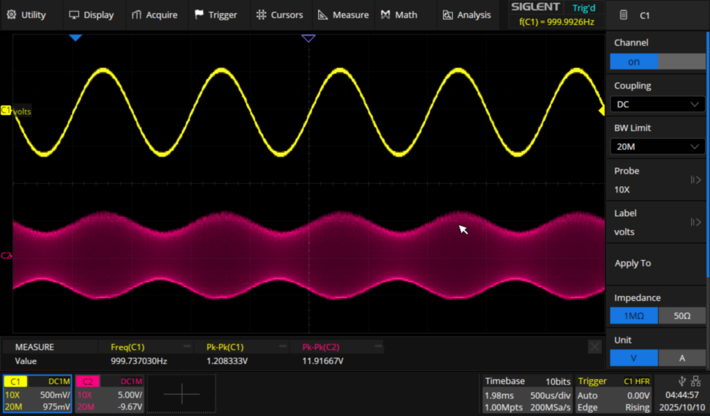
Here is our input modulating signal and the resultant modulation output after the high-pass output filter using discrete 2N3904 transistors. We were able to hear a reasonably pure tone that varied with modulation frequency once we finally found an AM radio to test it with.
Lab 5.3 Current mirror
The several current mirror circuits of §5L.3 pose a more difficult problem for substitution of the CA3096. All the current mirrors of this section rely on the assumption that two BJTs at the same temperature with the same base to emitter voltage will have identical collector current flows. However, even if the transistors you use to build the mirrors have very similar transconductance curves, the current in the mirrored transistor will differ from the programming transistor if their temperatures are not identical.
The lab starts with a current mirror built with discrete 2N3904 transistors (§5L3.1) and demonstrates how temperature differences between the reference BJT and the output transistor cause errors in the output current.
The solution in §5L.3.2.1 improves on the discrete version by using the thermally matched transistors in the CA3096 array to reduce temperature differentials between the devices. Without the transistor array you won’t be able to build this version, but it should be obvious after you have seen the change caused by temperature in the discrete version of the mirror in the previous section that using an array would improve temperature stability. Besides, as the book points out, you couldn’t actually show that worked since “we cannot repeat the temperature-mismatch experiment of §5L.3.1.1 … because we cannot force the two transistors’ temperatures apart. Instead, we’ll have to assume the temperature problem due to differential external heating on the two transistors is gone[.]” (You could, however, heat the CA3096 with your finger and see the output current not change by much to verify the benefit of the array.) However, if you want to build the current mirror with matched transistors you could use the NSS40301MDR2G dual match NPN transistors from onsemi and an SOIC-8 to DIP adapter for less than two dollars (see below).
The remaining circuits first demonstrate the Early Effect, which causes an increase in the output current as the collector-to-emitter voltage of the output transistor increases. While the text uses the CA3096 version of the current mirror in Figure 5L.26 as the starting point for the improved versions, the discrete version of Figure 5L.25 will work as well.
The Early Effect can be modeled as a high value resistor in parallel with the current source. When we tested the lab with discrete versions of the current mirrors, we measured values for the equivalent parallel resistance as follows
§5L.3.2.2 (simple current mirror) – 61.8k ohms
§5L.3.2.3 (mirror with emitter resistors) – 902k ohms
§5L.3.2.4 (Wilson mirror) – 1.6M ohms
showing the improvement gained with the more complex designs. These values were similar to those we measured using an actual CA3096.
So you can do all the experiments in Lab 5.3 using 2N3904 discrete transistors except §5L.3.2.1 where you replace the discrete BJTs in the simple mirror with an IC array.
If you want to see the improvement in the circuits with matched transistors and you are willing to solder surface mount devices onto a DIP carrier, the onsemi NSS40301MDR2G for $1.24 in a relatively easy to solder package using an SOIC-8 to DIP adapter works well. Only the base connected NPN pair (Q1 and Q2) need to be matched. Here is the Wilson current mirror of Figure 5L.27 built with the onsemi dual matched BJT:
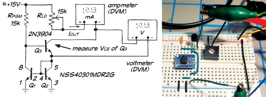
Using the NSS40301MDR2G dual matched BJT, we measured values for the equivalent parallel resistance as follows
§5L.3.2.2 (simple current mirror) – 66.1k ohms
§5L.3.2.3 (mirror with emitter resistors) – 1.28M ohms
§5L.3.2.4 (Wilson mirror) – 4.61M ohms