
Substitute for the LT1073 regulator on the analog parts list
Section 12L.2 invites readers of Learning the Art of Electronics to build both a boost (output voltage higher than input) and buck (output voltage is lower) switching voltage regulator using an LT1073 micropower DC-DC Converter. If you ever need a buck or boost converter in a project, the LT1073 and its sibling the LT1173 are wonderful devices. In the fixed-voltage version, you need only add an inductor, a diode, and a capacitor to the 8-pin DIP to get up to 40mA at 5V from a 1.25V source. In LAoE we use the adjustable version of the LT1073 which adds two resistors to allows us to set the output voltage to a value other than 5V or 12V. Unfortunately, the LT1073 is moderately expensive (USD$ 10.72 as of 5/2026). In addition, it hides the workings of a switching voltage converter. This is fine if you need one for a project but less ideal as a teaching exercise.
Luckily, by Chapter 11 LAoE readers have been introduced to almost all of the circuits in the blocks inside the LT1073. This means you can build the circuits in lab 11L.2 with parts you have already used (plus a MOSFET transistor on the analog parts list) and see how they go together to create a switching voltage regulator.[1] Here is an annotated version of the block diagram of the LT1073 showing discrete replacements for the circuits inside the device.
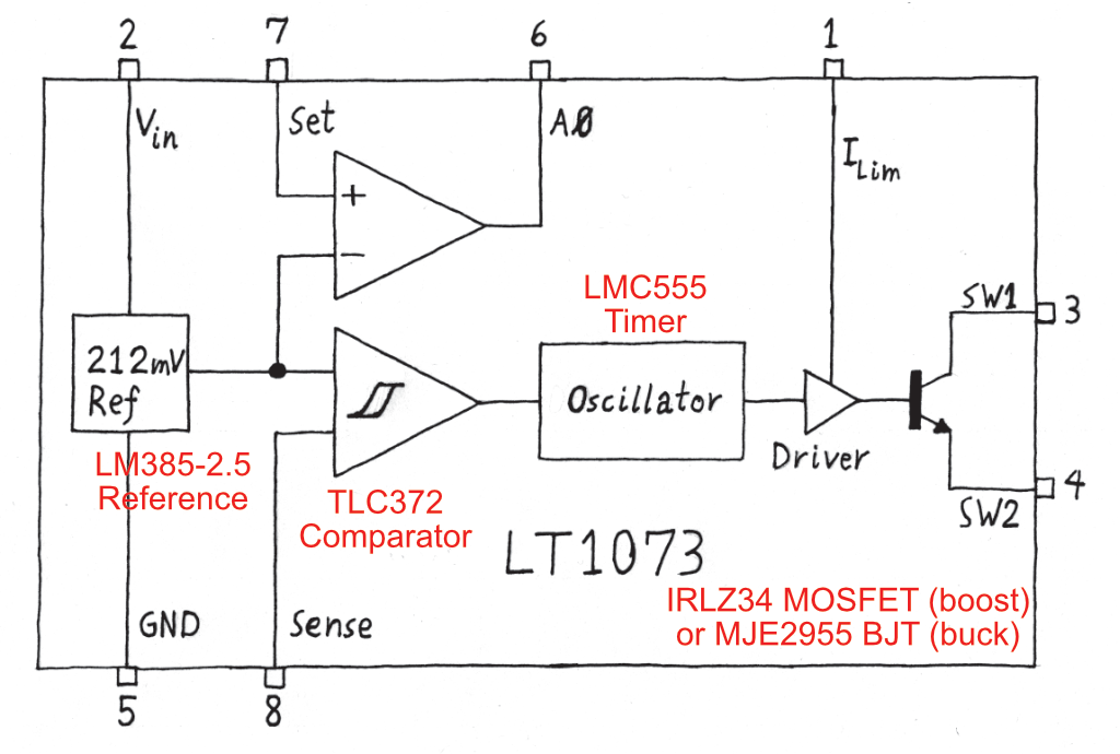
Annotated LT1073 block diagram showing the discrete circuits used to replace the device’s internal blocks. We don’t include the x1000 amplifier optionally used to reduce ripple in Figure 11L.13 but you could use a LMC6482 to replace it as well.
By building the circuits of 11L.2 out of separate components, you also gain the ability to look at the inputs and outputs of each of these blocks, something not possible with the integrated device.
11L.2.2 Step-up switching regulator replacement
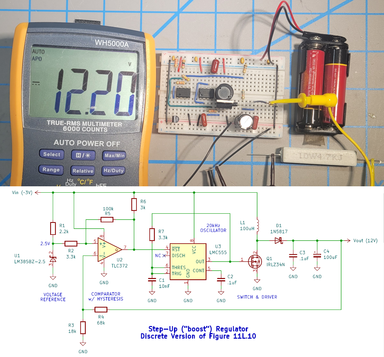
This circuit functions similarly to the LT1073 step-up converter in Figure 11L.10. However, it requires a 3V input (two AA cells) and outputs 12V.
Th circuit shown above operates almost identically to the LT1073 boost converter in Figure 11L.10. The LM385 supplies a constant 2.5V reference to the TLC372 comparator which is configured with hysteresis. When the output voltage divided by resistors R3 and R4 drops below 2.5V, the comparator output goes high (+3V) which enables the ~20kHz LMC555 oscillator. This drives the MOSFET on and off (think of it as a BJT switch that requires no base current). When the MOSFET is on, current builds up in the 100uH inductor. When the MOSFET turns off, the voltage at the drain (the pin marked “2”– similar to the collector of a BJT switch) rises until diode D1 forward biases and charges capacitors C3 and C4. (You saw a similar effect in lab 4L.6.2 using a BJT switch.) Once the output voltage reaches 12V, the comparator output goes low (0V) and turns off the oscillator. Unlike the LT1073, this circuit will not run on a single AA battery. While the the LMC555 will operate on a 1.5V supply, the LM385 reference requires at least a bit more than 2.5V to operate and the TLC372 has a minimum supply requirement of 3V. However, the basic operation of the circuit is the same.
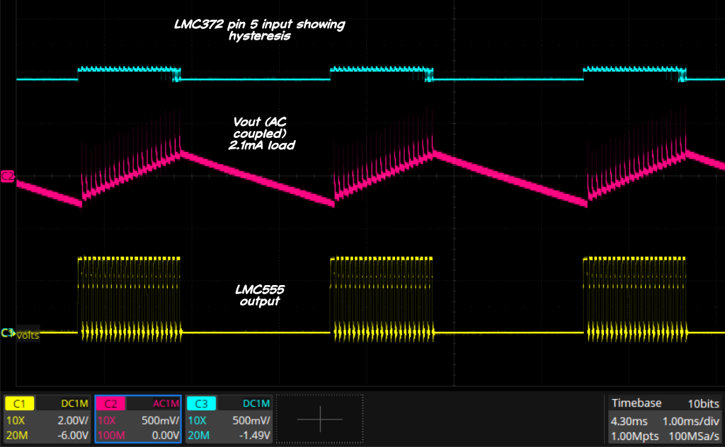
Step-up (boost) converter waveforms with a 4.7k load. At higher output currents, the LMC555 bursts would be closer together. At lower current, they would move farther apart.
Build the circuit shown above following the directions in lab 11L.2.2. Choose resistors R3 and R4 to give an output voltage of about 12V. You can use a standard 100uF electrolytic capacitor for C4 as we did; however, the noise on Vout will be reduced if you use the low ESR capacitor called out in the parts list. You should keep the output current under about 25mA for the test shown in Figure 11L.11.
11L.2.3 Step-down switching regulator replacement
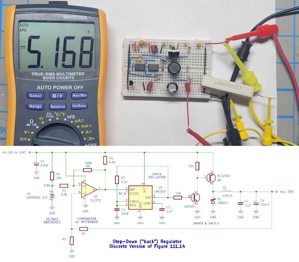
This circuit functions similarly to the LT1073 step-down converter in Figure 11L.14. However, the maximum allowed input voltage is limited to 15V by the LMC555 maximum rating.
This circuit implements the LT1073 configuration of Figure 11L.14. The TLC372 comparator output goes low (to ground) when Vout is too high, resetting the LMC555. This stops the 555 oscillating and sets its output to ground. This means the LMC555 must supply current to L1 to increase Vout when its output is high. However, switching transistor Q2 is on when its base is pulled down, so the 2N3904 transistor is included to invert the LMC555 signal.
While the LT1073 allows input voltages up to 30V, the input voltage for this circuit is limited to between ~6V (ours worked down to about 5.6V) and 15V, the maximum allowed VCC for the LMC555. Select R3 and R4 to provide a +5V output.
Unlike the boost circuit, where turning the output switch off creates the inductive kickback to generate a higher Vout than Vin , the buck configuration uses pulse width modulation to control the amount of energy that is supplied to the inductor when the switch is on. Diode D1 allows that energy to be transferred to the output once the switch turns off.
A downloadable PDF of the boost and buck LT1073 circuit schematics is available at https://laoe.link/misc/LT1073_Replacement_Circuits.pdf
[1] The only new item is the MOSFET transistor which we don’t get to until chapter 12. Feel free to skip ahead and read 12N.1.2 (it’s pretty short) if you are curious how it works.